
 Español
 English
 Français
 Português
 Deutsch
 Italiano
Optical Technology for On-the-Fly Robot AI Updates: Ending the Memory Bottleneck
1. Executive Summary
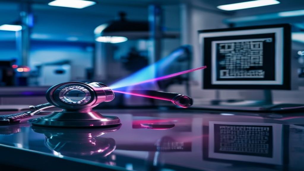
In a laboratory at Cornell University, a beam of red light emitted by an LED strikes an optical receiver placed nearly a meter away. The screen displays a matrix of squares reminiscent of a QR code, but it is not a simple web address. That burst of light is directly rewriting the device's memory, loading into it the parameters of an artificial intelligence model. The fundamental difference from any current system is that there is no intermediate analog conversion: the photocurrent generated by the light directly modifies the state of the memory.
This breakthrough, presented in July 2026 at the IEEE/JSAP Symposium on VLSI Technology & Circuits, addresses one of the most pressing problems in the AI industry: the data transfer bottleneck between memory and the processor. As language and vision models grow in size — with hundreds of billions of parameters — AI chips cannot hold all the information locally. The usual solution is to store parameters in DRAM and move them via electrical connections, a process that consumes enormous amounts of energy and limits scalability. The proposal by Yifan He, a postdoctoral researcher, and Jae-sun Seo, associate professor of electrical and computer engineering at Cornell Tech, eliminates that bottleneck at its root by using light to directly program the chip's memory. The potential impact is cross-cutting. It affects data centers that train and run models such as GPT-5.6 Sol from OpenAI, Claude Opus 5 from Anthropic, or Gemini 3.6 Flash from Google, where energy consumption due to data transfer is already a critical cost factor. It also reaches embedded systems such as autonomous robots, automated driving vehicles, and edge devices, where space and energy efficiency are even more severe constraints. For chip manufacturers, cloud infrastructure operators, and AI developers, this technology could redefine the rules of the game in the coming years.
2. In-Depth Technical Analysis
To understand the innovation, it is helpful to break down the traditional data flow in an AI system. A model like Llama 4 from Meta, with its 10 million token context, or DeepSeek-V4-Pro, specialized in code, requires storing billions of synaptic weights. These weights are stored in DRAM external to the compute chip. Every time the processor needs to access them — for example, during inference or retraining — the data travels through metallic electrical buses. That transfer is costly in energy and time, and it becomes the main limiting factor for large-scale performance.
Optical links, in theory, offer a solution: light can transport data at higher speed and with lower energy loss than copper wires. However, conventional optical receivers include analog-to-digital conversion (ADC) stages and transimpedance amplifiers that consume a significant portion of the energy. Those electronic circuits negate much of the advantage of optical transmission. This is where He and Seo's design comes in: their receiver does not translate light into electronic bits to later write them into memory; the photocurrent generated by the photons directly modifies the state of a memory cell. In practice, the system emits bursts of light forming matrix patterns similar to QR codes, but with much higher information density. Each light pattern represents a set of AI model parameters. The receiver, fabricated using standard CMOS technology, integrates photodetectors and memory cells on the same substrate. When light strikes, the generated current changes the conductance or voltage of the cells, thus writing the weight values without the need for intermediate conversion. This eliminates ADCs and amplifiers, drastically reducing energy per transferred bit.
One of the most relevant aspects is that the receiver can update the memory while the rest of the system continues operating. That is, an autonomous robot encountering a new situation could receive the parameters of a recalibrated model "on the fly," without needing to stop its operation or consume the energy that a conventional electrical download would entail. This opens the door to AI systems that adapt in real time to changing environments without interruptions.The proposal also addresses the scalability problem. As models grow, the number of parameters that must be transferred from DRAM to the processor becomes a funnel. With direct optical links to memory, multiple receivers could work in parallel, simultaneously loading different parts of the model. This would allow, for example, a data center to run inferences on models like Claude Opus 5 or Qwen 3.7-Max with a fraction of current energy consumption.
From a technological maturity standpoint, the researchers have demonstrated the concept in a laboratory prototype. Integration at production scale remains to be solved, as does the standardization of light patterns (equivalent to an "optical weight protocol") and compatibility with current manufacturing processes. However, the fact that the receiver uses standard CMOS technology is a very favorable factor for its eventual commercialization.3. Industry and Market Impact
The first sector to be affected is that of hyperscale data centers. Companies such as Google, Microsoft, Meta, Amazon, and emerging Chinese firms (DeepSeek, Qwen, Kimi) are investing billions in infrastructure to run ever-larger models. It is estimated that between 30% and 40% of the total energy consumption of an AI server is due to data movement between DRAM and the processor. If direct optical transmission to memory manages to cut that figure in half — and the researchers' own estimates suggest it could be even lower — the savings in operating costs and carbon emissions would be massive.
For chip manufacturers such as NVIDIA, AMD, Intel, and new Chinese players (like those producing Xiaomi's MiMo-V2-Pro chip), the technology represents both a threat and an opportunity. Current GPU and AI accelerator designs rely on high-speed electrical interconnects (such as NVLink or PCIe). If an optical receiver integrated into the chip die itself allowed parameters to be loaded directly into local memory, the need for those complex and costly buses would be reduced. On the other hand, companies that first adopt this technology could gain a significant competitive advantage in energy efficiency. In the realm of robotics and autonomous systems — from automated driving cars to delivery drones — the ability to update AI models without interruptions and with low power consumption is revolutionary. Today, an autonomous vehicle needs to periodically download new maps or perception parameters, a process that consumes battery and processing time. With direct optical memory, those updates could be carried out via bursts of light, almost instantaneously, while the vehicle continues moving. The edge computing market would also benefit. Devices such as industrial sensors, wearables, or smart home assistants operate on very tight energy budgets. Being able to retrain or update a lightweight model — such as Gemini 3.6 Flash from Google, a 12-billion-parameter model designed for edge computing — via an optical signal would eliminate the need for high-power wireless connections or physically replacing the storage module. However, there are barriers. The industry is highly standardized around electrical interconnects and memory protocols such as DDR, HBM, or GDDR. Migrating to an optical scheme will require agreements among chip manufacturers, system designers, and data center operators. It is likely that initial deployments will occur in very specific niches, such as supercomputing or proprietary data centers of large tech companies, before becoming widespread.
4. Expert Perspectives and Strategic Analysis
"People are designing all kinds of different AI chips," said Jae-sun Seo during the presentation at the symposium. "These processors often lack space for all the parameters that make up AI models, so additional data is stored in DRAM. The electrical connections used to move that data between DRAM and the processor create cost and efficiency problems as systems scale. That's one of the main bottlenecks." Professor Seo's quote clearly summarizes the problem his team is addressing.
Industry analysts agree that the Cornell Tech solution attacks a critical point that no previous proposal had resolved so cleanly. Previous attempts to use optics for AI interconnects focused on optical links for chip-to-chip communication, but still required electronic conversion at the endpoints. The write-directly-to-memory receiver avoids that conversion, representing a conceptual leap. From a strategic standpoint, companies should consider several lines of action. First, OEMs and chip designers should initiate collaborations with research groups like Cornell Tech to evaluate the feasibility of integrating these receivers into future accelerator generations. Second, data center operators should budget R&D funds for direct-to-memory optical interconnect prototypes, with an eye toward potential implementation within the next 3 to 5 years. Third, robotics and autonomous vehicle startups should closely monitor these developments, as they could be the first to adopt the technology in high-value commercial products. The geopolitical context must also be considered. China, through its AI companies such as DeepSeek, Qwen, and GLM, is investing heavily in alternative hardware to circumvent advanced chip export restrictions. A technology like this, which does not rely on extremely fine lithography (it can be implemented in standard CMOS), could be especially attractive to the Chinese ecosystem. It would not be surprising to see similar announcements from Chinese universities or companies in the coming months. Finally, the technical consensus points to write speed as the main challenge. The light bursts must be fast enough to match or exceed the bandwidth of current electrical interconnects (hundreds of GB/s). The demonstrated prototype operates at laboratory speeds, but scaling to gigahertz frequencies will require optimizing both the photodetectors and the memory cells. This is an engineering problem, not fundamental physics, and therefore addressable with adequate resources.
5. Roadmap and Predictions
In the short term (2026-2027), we will see intensified research in this field. Seo and He's group will likely publish more detailed results on achieved bandwidth, error rate, and durability of memory cells under repeated optical writing. It is also expected that other laboratories — both academic and corporate, including those of Google, IBM, and the Chinese giants — will enter the race to optimize the concept.
In the medium term (2028-2029), the first pre-commercial prototypes integrated into test chips could appear. These will likely be initially targeted at supercomputing and data center applications, where energy savings justify investment in new infrastructure. Cooling systems would also benefit, since the reduction in heat generated by electrical interconnects would allow higher compute densities. Toward 2030, if the technology matures, it could become a de facto standard for parameter transfer in large AI models. By then, neuromorphic processors and in-memory computing architectures could naturally integrate optical receivers as weight input peripherals. Autonomous robots, vehicles, and edge devices would be the first commercial beneficiaries, followed by hyper-scale data centers. There is a possibility that a bidirectional variant will emerge: not only writing parameters to memory, but also reading memory state via light, enabling a true full optical interface. This would further accelerate chip-to-chip communication and open up new distributed computing architectures.
6. Conclusion: Strategic Imperatives
The technology presented by Cornell Tech researchers is not an incremental improvement; it is a paradigm shift in how AI systems access their parameters. By eliminating intermediate analog conversion and allowing light to write directly into memory, it attacks the root of the energy problem limiting the scalability of current models. At a time when frontier models — GPT-5.6 Sol, Claude Opus 5, Gemini 3.6 Flash, DeepSeek-V4-Pro — consume enormous amounts of energy, any advance that reduces the cost of data movement has a direct impact on the economic and environmental viability of AI.
For ecosystem players, the immediate actions are clear: hardware R&D departments should establish contact with the Cornell Tech team and begin evaluating the integration of optical receivers into their roadmaps. Data center operators should closely monitor reliability and performance results. And developers of robotics and edge applications should prepare for a future where model updates require neither cables nor high power consumption, but simple flashes of light. The memory bottleneck has for years been the Achilles' heel of artificial intelligence. If this optical technology becomes established, that bottleneck could become history. The question is no longer whether light will replace copper in critical AI interconnects, but when and who will take the first step to commercialize it at scale.