 Español
 English
 Français
 Português
 Deutsch
 Italiano
AI Is Giving Optical Computing a New Lease on Life
 AI-generated
1. Context and Key Points
For the past decade, optical computing remained an academic curiosity, limited to research laboratories and lab demonstrations. However, starting in 2022, the pressure from AI inference, which consumes more energy than most data centers combined, has turned photonics into a potentially disruptive solution. The market for companies dedicated to light-based computing has expanded from $0.4 billion in 2022 to $2.22 billion in 2023, and analysts project exponential growth over the next five years.
The decisive factor is the ability of light to perform matrix operations and Fourier transforms with substantially lower energy consumption than traditional CMOS circuits. While completely replacing GPUs like those from Nvidia remains an ambitious goal, the integration of optical modules into the data chain, for example, in network switches or inference accelerators, is already demonstrating energy cost reductions of 30% to 50% in benchmark tests.
The readers who should pay attention are CTOs of data centers, hardware R&D directors, semiconductor technology investors, and sustainability policy leaders in the AI industry.
2. Key Technical Aspects
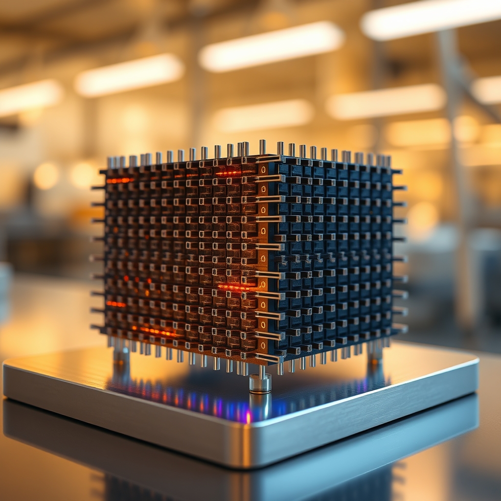
Optical computing is based on the manipulation of photons to perform linear operations, primarily matrix multiplications and Fourier transforms. In a photonic chip, data is encoded in the phase or amplitude of light pulses that traverse a network of programmable interferometers (MZI, Mach-Zehnder interferometers). Each MZI acts as an analog logic gate that, when combined, implements the multiplication of a dense matrix.
The critical advance in recent years has been the integration of high-speed electro-optic modulators (over 50 GHz) and CMOS-compatible photonic detectors. These components allow the latency of an optical operation to be on the order of nanoseconds, comparable to the latency of a GPU memory operation, but with energy consumption reduced to tens of microwatts per operation.
A second pillar is the "in-network computing" architecture. Companies specializing in photonics are inserting optical modules directly into the data switching path of data centers. Their basic element is an on-chip Fourier transform calculator, which allows convolutions and filters to be executed directly on the optical signal already circulating through the network. By avoiding electro-optic-electro conversion, a significant source of energy loss and latency is eliminated. From an AI architecture perspective, optical computing is well-suited to inference models that rely on dense and convolutional layers. Model weights can be stored in static optical matrices (for example, using programmable diffraction gratings) and reused without the need to reload data from DRAM memory, which reduces pressure on HBM bandwidths. However, photonics presents limitations. The typical numerical precision of optical modules is in the range of 8-bit or 4-bit, which necessitates aggressive quantization techniques. Additionally, the linearity of modulators and the thermal stability of the chip are manufacturing challenges that still require stricter quality control processes than those for CMOS circuits. In the research field, groups from Cornell, MIT, and the University of Southampton have demonstrated complete neural networks in optical hardware, achieving inference rates of several tera-operations per second (TOPS) with power consumption of less than 10 W. These lab tests confirm theoretical viability, but the transition to production requires the standardization of programming interfaces (for example, extensions to CUDA or OpenCL kernels) and integration with existing AI software stacks. Finally, the convergence of photonics with quantum computing is emerging as a parallel research path. Photons can serve as qubits in optical quantum computing platforms, opening the possibility of accelerating hybrid algorithms that combine classical and quantum AI.
3. Industrial Impact and Market Repercussions
The jump from $0.4 billion to $2.22 billion in market valuation reflects a wave of funding rounds led by venture capital funds specialized in high-performance hardware. In the U.S., Lightmatter and LightOn (headquartered in France but with a strong presence in the U.S. market) have raised more than $300 million combined since 2022. In China, companies in the sector have secured significant financing, while in Israel, sector startups have attracted strategic investment.
For cloud infrastructure providers, the adoption of optical modules represents a path to meeting CO₂ emission reduction targets. According to an internal study by a major cloud operator, replacing 10% of inference GPUs with optical accelerators would reduce the total energy consumption of the data center by approximately 15% and operational costs by a range of 5% to 8%.
Traditional semiconductor manufacturers are responding with strategic alliances. Intel has announced a collaboration with Lightmatter to integrate optical modulators into its Xeon processor line, while Samsung is exploring the co-fabrication of photonic detectors in its 3 nm process. In the telecommunications sector, the insertion of optical computing into the switching layer allows for the provision of "edge" inference services directly on the fiber network, reducing the perceived latency for computer vision and natural language processing applications on IoT devices. The software ecosystem is also evolving. Frameworks like PyTorch and TensorFlow are incorporating photonic backends through low-level APIs, which facilitates for developers to port existing models without rewriting the code.
| Year | Market Valuation (USD billions) |
|---|---|
| 2022 | 0.4 |
| 2023 | 2.22 |
4. Market Perspectives
Researchers at Cornell University argue that "most of the interest in photonics is driven by the fact that AI inference has been literally limited by power." Their assessment is based on energy consumption measurements in large-scale model training clusters, where the energy dedicated to the compute layer exceeds 70% of the total.
Industry analysts agree that optical computing will not immediately replace GPUs, but it will redefine the architecture of inference systems. An emerging consensus suggests a hybrid strategy: GPUs for non-linear operations (activations, normalizations) and optical modules for the linear part (matrix multiplications). This combination maximizes efficiency without requiring a complete rewrite of the software stack.
From the investors' perspective, the key lies in the ability to scale the production of photonic chips. 193 nm photolithography remains the dominant process, but the adoption of 3D packaging techniques and silicon-photonics (SiPh) interconnection is reducing manufacturing costs. Venture capital funds are prioritizing startups that demonstrate a clear roadmap toward production volumes of thousands of units per month. Energy and environmental regulators are beginning to consider photonics as an option to meet carbon neutrality commitments. In the European Union, energy efficiency directives include references to low-consumption technologies, which could translate into tax incentives for operators adopting optical accelerators. Regarding competition, Nvidia has announced its roadmap to include optical interconnection modules in its next-generation GPUs. Although the company has not revealed technical details, the initiative indicates that GPU leaders are taking the threat of photonics seriously and are seeking to integrate the technology into their own ecosystems.
5. Next Steps
In the 2024, 2025 horizon, the first optical inference modules are expected to be available as PCIe cards for high-performance servers. These cards will offer a performance of 1 TOPS/W, sufficient to run language models of up to 7 billion parameters with energy consumption less than 40% of an equivalent GPU.
For 2026, 2027, the trend will be the integration of optical modules directly into the architecture of server chips, via 2.5D packaging that combines silicon and photonics in the same interposer. This generation will allow sub-microsecond latencies in data transmission between HBM memory and the optical accelerator.
In the 2028, 2030 period, the convergence of optical computing with large-scale generative AI (models of more than 100 billion parameters) will be the driver of massive adoption. Data centers implementing hybrid networks will be able to reduce their total energy consumption by more than 30% and, at the same time, offer response times that meet the requirements of augmented reality and autonomous vehicle applications. In parallel, the standardization of programming interfaces will facilitate interoperability between providers and accelerate adoption in the developer community.
6. Conclusion and Assessment
Optical computing has moved from being an academic curiosity to a viable commercial solution, driven by the energy crisis of AI inference. Technology leaders must evaluate the incorporation of optical modules into their infrastructures gradually, starting with linear-intensive workloads and network environments where light is already the transmission medium.
The immediate imperatives are three: first, initiate pilot tests with available optical accelerators in PCIe format to validate cost and energy savings; second, establish alliances with photonics providers that offer scale production guarantees; and third, update software stacks to support optical backends, ensuring that development teams receive adequate training.
Ultimately, the strategic adoption of photonics will not only mitigate the energy bottlenecks of AI but also position organizations at the forefront of a new era of high-efficiency computing.