 Español
 English
 Français
 Português
 Deutsch
 Italiano
OpenAI Assists AMD in Improving Next-Gen Flagship GPU Design by 14% PPA and Powers Lisa Su's New Processors
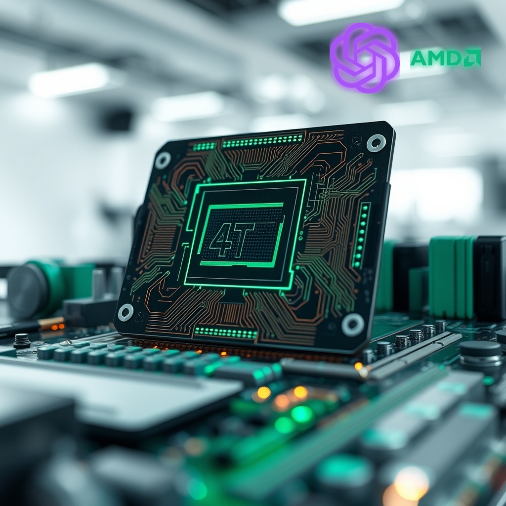 AI-generated
1. Context and Highlights
The semiconductor industry is undergoing a structural transformation where the design complexity of advanced nodes exceeds the capabilities of traditional manual optimization. In this context, a recent strategic collaboration between OpenAI and Advanced Micro Devices has demonstrated that large language models can drastically accelerate integrated circuit engineering. Using specialized variants of GPT-like architectures, Lisa Su's team at AMD successfully optimized the physical design and logical layout of their upcoming flagship GPU, achieving a 14% improvement in the PPA metric, which encompasses power, performance, and silicon area.
This breakthrough is not limited to the high-end graphics accelerator, but extends its impact to the company's new generations of central processors. The integration of artificial intelligence-assisted workflows into automated circuit design represents a paradigm shift for the semiconductor industry. By reducing design cycles and mitigating thermal and electrical bottlenecks, silicon companies can accelerate their time to market and compete more effectively in a market dominated by a scarcity of specialized engineering resources and constant pressure for energy efficiency.
For chief technology officers and system architects, this case study transcends a simple corporate anecdote and consolidates as empirical proof that generative artificial intelligence is already an indispensable tool in physical hardware design. The competitive implications compel a reevaluation of chip development roadmaps across the global ecosystem, placing algorithmic optimization at the same level of importance as advanced lithography technologies such as extreme ultraviolet photolithography.
2. Key Technical Aspects
Designing a modern integrated circuit with billions of transistors involves solving combinatorial problems of unprecedented complexity. The placement of logic blocks, the routing of the power delivery network, and the minimization of parasitic capacitance are tasks that traditionally consume months of human and computational iteration. In the development of AMD's new flagship GPU, OpenAI models' intervention focused on guiding placement and routing algorithms using reinforcement and deep learning, identifying spatial configurations that conventional heuristic optimizers missed due to their local focus.
The 14% improvement in PPA is broken down into three fundamental vectors for the silicon architecture. First, the reduction of dynamic and leakage power was achieved through a more efficient arrangement of standard cells around the floating-point calculation blocks and high-bandwidth memory controllers. Second, overall performance benefited from a decrease in the length of critical interconnections, which reduced the resistance and capacitance of the copper tracks, enabling higher clock frequencies without exceeding the thermal margins allowed by the packaging.
Third, the optimization of the silicon area allowed functional blocks to be densified without compromising structural integrity or increasing the wafer defect rate. This assisted design process did not operate in isolation, but was deeply integrated into the commercial electronic design automation tools used by AMD engineers. The models analyzed terabytes of data from previous electrical simulations to predict the thermal and electromechanical behavior of the chip before performing the first tape-out, a milestone that drastically reduces the manufacturing costs of defective prototypes.
The application of this methodology to AMD's new CPUs demonstrates the versatility of language models across different architecture domains. While GPUs prioritize parallel density and massive bandwidth, CPUs require rigorous optimization of cache latency and branch prediction at the microarchitectural level. The ability of artificial intelligence systems to reason about complex decision trees and data dependencies made it possible to refine interrupt buses and cache coherency controllers, achieving incremental performance-per-watt gains that would have required multiple physical iterations.
This level of computational optimization highlights the convergence between machine learning research and semiconductor hardware engineering. The underlying infrastructure required massive compute clusters capable of processing thermal fluid dynamics simulations and signal integrity analyses in parallel with model inferences. Far from being a static process, the workflow involved a continuous feedback loop where each physical simulation fed back into the model embeddings to fine-tune subsequent predictions.
The technical challenges overcome during this collaboration included managing the enormous volume of data generated by electronic design automation tools and the need to maintain accuracy in transistor-level simulations. The models' ability to process massive contexts facilitated the correlation between high-level architectural specifications and sub-micron physical constraints, a bridge that has historically required the manual intervention of senior engineers over months of work.
3. Industry Repercussions
The announcement of this collaboration shakes the foundations of the semiconductor industry and alters the competitive landscape among major manufacturers of processors and artificial intelligence accelerators. AMD, under the leadership of Lisa Su, once again demonstrates its operational agility by adopting disruptive technologies in its internal design workflows, narrowing the gap against traditional competitors that rely exclusively on proprietary methodologies. This alliance underscores that even the most advanced hardware companies find incalculable strategic value in adopting frontier models developed by specialized software and artificial intelligence laboratories.
For the enterprise ecosystem, the message is clear: competitive advantage in the era of intelligent systems no longer resides solely in access to the most advanced lithography machines, but in the efficiency with which the circuits printed on them are designed. A 14% improvement in PPA on a cutting-edge node can translate into a differential performance advantage over the competition, allowing for greater computing power per watt in data centers and edge devices. This puts pressure on other market players to replicate these artificial intelligence-assisted design practices so as not to fall behind in the race for energy efficiency.
The electronic design automation tool market is also undergoing a strategic realignment. Traditional design software vendors must integrate large language model capabilities into their platforms to meet the demand for intelligent workflows. Semiconductor companies that manage to build or license internal AI capabilities applied to silicon will gain unprecedented design autonomy, reducing their dependence on standard industry methodologies and optimizing their research and development budgets.
At the macroeconomic level, the optimization of design processes through artificial intelligence helps mitigate the exponential increase in the cost of manufacturing semiconductors at advanced nodes. By reducing the number of iterations required to obtain a functional and marketable design, engineering resources are optimized and the financial risk associated with the development of new silicon chips is minimized. This partially democratizes access to the creation of custom chips, allowing more organizations to explore specialized architectures for specific workloads.
4. Market Perspectives
Industry analysts agree that the collaboration between OpenAI and AMD marks a turning point in the industrial symbiosis between artificial intelligence software and the physical infrastructure that supports it. The ability of models to act as advanced copilots in complex engineering tasks demonstrates that artificial intelligence has moved beyond the superficial experimentation phase to integrate into the mission-critical operational cores of tech companies.
From a corporate strategy perspective, AMD's decision to collaborate with an artificial intelligence leader to improve its own hardware illustrates a trend toward cross-sector co-innovation. Chip manufacturers can no longer be considered entities isolated from the software ecosystem; the joint optimization of silicon and algorithms maximizes the overall performance of artificial intelligence workloads.
Engineering directors and CTOs in the hardware industry are advised to immediately evaluate the integration of language model-assisted design workflows into their internal processes. Resistance to methodological change or exclusive reliance on traditional electronic design automation tools are emerging as serious operational risks in a market moving toward automated algorithmic optimization.
Furthermore, it is essential for organizations to develop internal talent capable of bridging the gap between semiconductor engineering and machine learning. The scarcity of hybrid profiles who understand both semiconductor physics and transformer model architecture represents the greatest bottleneck to the mass adoption of these techniques across the entire industrial ecosystem.
5. Future Outlook
The evolution of AI-assisted chip design methodologies points towards increasingly deep automation over the coming years. By the end of the decade, human intervention in the initial phases of placement and routing of logic blocks is expected to be drastically reduced, allowing artificial intelligence systems to generate and verify complete architectures from high-level functional specifications.
In the short term, upcoming iterations of design flows from AMD and other manufacturers will integrate multimodal capabilities capable of interpreting complex schematic diagrams, natural language architecture specifications, and physical constraints simultaneously. This will further accelerate development cycles, enabling weekly design iterations instead of monthly ones.
In the medium term, the convergence between silicon optimization and the execution of language models at the edge will drive the development of hardware architectures specifically designed to accelerate the inference and training processes used in chip design itself. This self-referential feedback loop will consolidate a cycle of continuous improvement in the semiconductor industry.
6. Conclusion: Strategic Imperatives in the Design of AMD's New Flagship GPU
The 14% PPA optimization achieved by AMD in its upcoming flagship GPU through technical collaboration with OpenAI consolidates a new era in semiconductor engineering. Artificial intelligence is no longer just the workload executed by chips, but the intellectual tool that enables the design of AMD's new flagship GPU with a level of efficiency unattainable by the human mind in isolation.
For industry leaders, the strategic imperative is clear: the adoption of advanced language model-based workflows for hardware optimization, especially for high-performance graphics accelerators, is an inescapable necessity. Companies that integrate these capabilities into their engineering processes will maintain a sustainable competitive advantage in the development of AMD's next flagship GPU and related architectures, while those that cling to traditional methodologies will face operational obsolescence in an increasingly demanding semiconductor market.